
Silicon Carbide 3D Printing
What Is Silicon Carbide?
Silicon Carbide (SiC) is an advanced ceramic material prized for its exceptional combination of mechanical, thermal, and optical properties. It's extremely hard and wear-resistant, maintains its strength at high temperatures, resists chemical attack, and has a high thermal conductivity paired with a very low coefficient of thermal expansion. That last combination — moving heat efficiently while barely changing shape as temperatures shift — is what makes SiC so valuable in applications where dimensional stability is critical, from aerospace components to semiconductor processing equipment to precision optical systems.
These same properties, however, make silicon carbide notoriously difficult to manufacture. Its hardness and brittleness make conventional machining slow, tool-intensive, and prone to cracking or chipping, especially in complex geometries.
The Benefits of Additively Manufactured Silicon Carbide
Additive Innovations uses binder jetting to 3D print Silicon Carbide powdered material, offering a compelling alternative to conventional manufacturing methods like casting and machining. Binder jetting builds SiC parts layer by layer directly from powder, and that fundamentally different approach delivers advantages that traditional processes struggle to match:
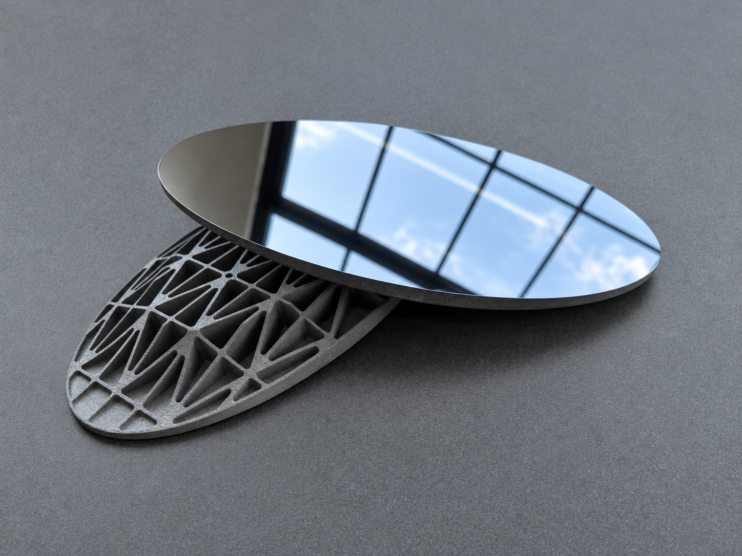
Design freedom — Binder jetting can produce complex internal geometries — lattice structures, lightweighting cavities, and non-uniform cross-sections — that are difficult or impossible to machine conventionally. This opens the door to SiC components optimized for weight and stiffness rather than constrained by what a cutting tool can reach.
Reduced material waste — Machining SiC from solid stock is inherently subtractive, removing (and wasting) significant material to reach a final shape, on a material that is expensive and hard to source. Binder jetting uses only the powder needed to build the part.
Lower tooling investment — Casting SiC typically requires part-specific molds and tooling, adding cost and lead time for every new geometry. Binder jetting is a tool-less process, allowing new designs to move to production without new mold investment.
Faster design iteration — Because no new tooling is required, design changes can move from concept to physical part far faster than with casting or machining, accelerating development cycles.
Reduced risk of machining-induced defects — SiC's hardness and brittleness make it prone to microcracking and surface damage during conventional machining. Building near-net-shape via additive manufacturing reduces the amount of post-process material removal required, lowering the risk of introducing defects.
Design consolidation — Multiple components that would otherwise need to be machined separately and assembled can potentially be printed as a single part, reducing joints, fasteners, and points of failure.
While Additive Innovations' principal focus has been optics — our binder jetting capability extends to printing Silicon Carbide in a wide range of forms and geometries, supporting SiC applications well beyond optics.
Silicon Carbide Optics
Silicon Carbide has become a material of choice for precision optical systems, particularly in demanding environments like space telescopes, airborne and ground-based astronomical instruments, and high-performance imaging systems. Its high stiffness-to-weight ratio allows optical mirror substrates to be lightweighted without sacrificing rigidity, while its low thermal expansion ensures the mirror's shape — and therefore its optical performance — remains stable even as the operating environment's temperature shifts. SiC's high thermal conductivity further helps optical systems reach thermal equilibrium quickly and evenly, minimizing distortion caused by temperature gradients across the mirror surface.
These characteristics have made SiC a preferred substrate material for mirrors used in aerospace, defense and other commercial applications where dimensional stability under extreme or fluctuating conditions is essential — and where the ability to produce lightweight, complex substrate geometries through additive manufacturing offers a real advantage over conventionally manufactured alternatives.
Silicon Carbide Material Properties Summary
| Density | Flexural Strength | CTE | Thermal Conductivity |
|---|---|---|---|
| 2.7-2.9 g/cc | 200-300 MPa | 2.3-2.4 ppm/°C | 100-150 W/m-K (RT) |
Working With Additive Innovations

Our Process:
1 - You provide us with your 3D design file in a common file format (.obj, .stl)
2 - We print your substrate leveraging our proprietary binder jet AM process
3 - We infiltrate your substrate to produce a fully dense Si-SiC part
4 - Your substrate is ground and polished to produce a final optic
Silicon Carbide Development Examples Completed by Additive Innovations
3D Printed Silicon Carbide For HEL Directed Energy
Lightweight Silicon Carbide Mirrors via Binder Jet Additive Manufacturing
Additive Manufacturing of High-Precision, High-Numerical Aperture Silicon Carbide Optics
Low-Cost, Free-Form Optics Using Silicon Carbide Additive Manufacturing
Request a Quote
Send your part file today and one of our applications engineers will get back to you within 24 hours.
Typical lead times are approximately four weeks; expedited orders may be ready in as little as one week.
